We all know that gateway is a digital logic circuit, when combined, we can perform simple logical operations on data. In this post, we will discuss the model of the NOR gate from top to bottom and bottom to top. The following figure shows the basic NOR gateway, Gate Level Modeling, Data Flow Modeling, Behavioral Modeling, RTL Simulation and NOR Truth Table
NOR Gate
OR Gate symbol
The NOR Gate have 2 input and a single output where A, B are the inputs and Y is the output. In NOR Gate, the output will be High only if both inputs are low (0)
The boolean equation of a NOR gate is Y = (A + B)’.
Input A | Input B | Output y |
0 | 0 | 1 |
0 | 1 | 0 |
1 | 0 | 0 |
1 | 1 | 0 |
Truth Table
Gate Level Modeling
Designing circuits using basic logic gates is known as a gate-level model. Since gates are an integral part of any logic design, gate primitives can be used to create complex level concepts such as multiplexers, and encoders.
The first items described in Verilog are set keeping the user's needs in mind making it easy to design large blocks. Gate level analysis also takes care of possible gate delays at the highest output level. Most of the time we do not look at the delays caused to the circuit due to the gates.
Designers can create low-level models from high-performance models automatically or automatically. The process of automatically generating a gate-level model from a data stream or a behavioural model is called Logic Synthesis. Verilog supports defining circuits using logical gates as pre-defined elements. Primitives are validated as modules unless otherwise specified in the Verilog syntax and do not require module definitions.
NOR Gate is a Universal Gate. NOR Gate has two inputs A, B and a single output Y. When both inputs are 0 0 output is 1 when one input is 0 and another input is 1 then the output is 0 when one input is 1 and another input is 0 then the output is 0 and when both inputs are 1 the output will be 0
module Nor_Gate(y,a,b );input a,b;output y;nor (y,a,b);endmodule
Data Flow Modeling
Compared to gate-level modeling, data flow modeling makes for a more ambiguous meaning. Dataflow modelling defines circuits for their function instead of their gate structure. The module is used to determine how data flows between registers. That is very useful because modelling at the gate level becomes very difficult for large circuits.
Data flow modeling is therefore a very important way to use design. This design style requires continuous assignment statements. Ongoing activities are done using the keyword assign.
Instead of using directly in data flow we use operations such as & (Bit-Wise AND), * (Multiply), % (Modulus), + (Plus), - (Minus) && (Logical AND) etc in Data Flow modelling . Verilog provides 30 different types of Operators. It is used to describe combinational circuits.
module Nor_Gate_Data_Flow(a,b,y);input a,b;output y;assign y = ~(a|b);endmodule
Test Bench
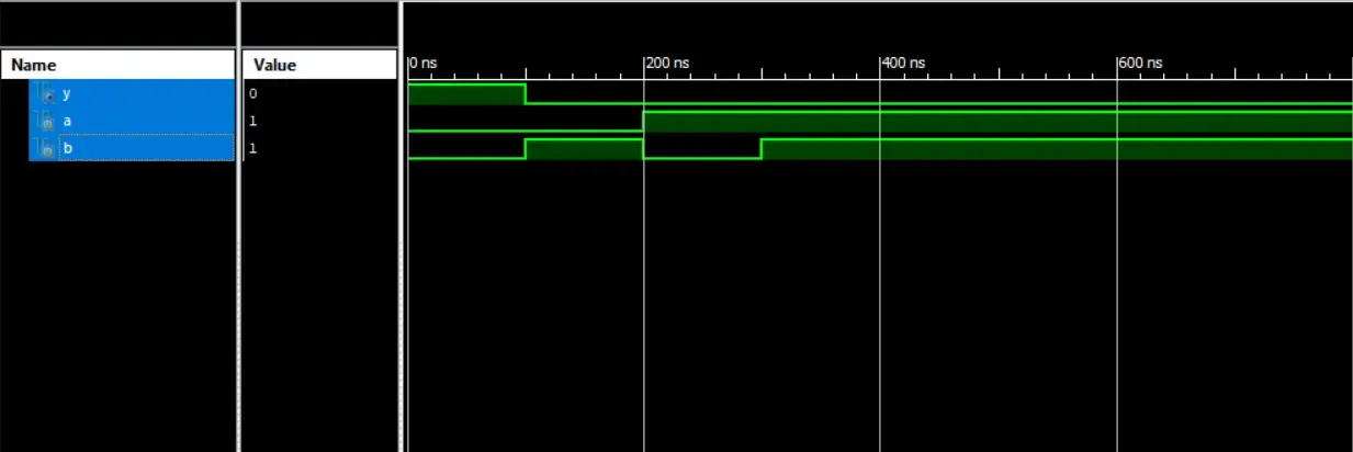
The code shown below is the test bench for NOR Gate. It is used to give values for Input of NOR Gate. Here a=0; b=0; represent the values of input at A and B. #100 represents the wait time. So that we can get a clear waveform in RTL simulation
module Nor_Gate;// Inputsreg a;reg b;// Outputswire y;// Instantiate the Unit Under Test (UUT)Nor_Gate_Flow uut (.a(a),.b(b),.y(y));initial begin// Initialize Inputsa = 0;b = 0;#100 a=0;b=1;#100 a=1;b=0;#100 a=1;b=1;// Wait 100 ns for global reset to finish#100;// Add stimulus hereendendmodule
RTL Simulation
Here we represent Register Transfer Level (RTL) For NOR Gate for both Data Level and Data Flow modelling.
By looking at waveforms, we can find that whenever the inputs of both A and B are low then the output is high, if not in all other cases the output is low. By checking the above waveform we can determine whether our waveform is right or wrong by comparing it with the truth table given above. This waveform has to match with the same truth table of NOR Gate.
Read Also
Tags
Share to other apps


